Introduction to Multilayer Surface Mount Inductors
Multilayer chip inductors were introduced in 1987 and soon became the inductive components of choice for many design engineers. Multilayer technology offers three advantages:
- Monolithic structure — excellent for high reliability
- Magnetic shielding — outstanding for very high density applications
- Low mounting cost
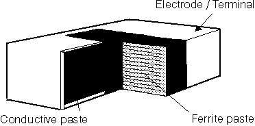
Construction of Multilayer Chip Inductors
Multilayer chip inductors do not require winding. They consist of ferrite paste and conductive paste alternately layered and sintered in a monolithic structure. The process can be described as follows:
- First a ferrite paste and a conductive paste are printed. This is the starting point of the conductor.
- Another ferrite paste and conductive paste are printed, and connected to the conductor pattern.
- Another ferrite paste and conductive paste are printed, completing the conductor pattern.
- Last ferrite paste is printed.
- Co-firing.
- Terminal / electrode processing.
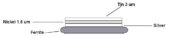
Terminal Electrode Construction
Soldering
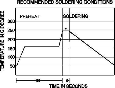
Multilayer chip inductors are designed for flow or reflow soldering methods only. All chips should be pre-heated at a temperature of 150° C for 60 seconds. Flow and reflow should be done at 245° C for 0.5 seconds, with rosin flux (chlorine less than 0.20% wt.).
If using soldering iron, the following conditions must be met:
- Soldering iron — 30 Watts maximum
- Tip temperature — 300° C maximum
- Soldering time — 3 to 5 seconds maximum
Cleaning
Vapor degreasing and water detergent rinse are the cleaning methods we recommend. Be sure to completely remove all flux residue. Some cleaning agents may change the color of the chip body to slightly white; however, product performance is not affected.
For additional help with cleaning components, contact ACT’s engineering department.
Storage
All multilayer chips should be stored on tape and reel. We do not recommend bulk storage of these parts. Do not expose reels to prolonged heat or direct sunlight. Do not store in relative humidity higher than 65%. Avoid areas that have sudden changes in temperature and humidity. Do not store components in a chemical atmosphere such as chlorine gas, acid or sulfide gas.
Land Pattern Design
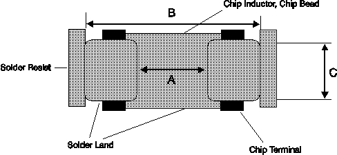
Land Pattern Design. Dimensions in mm.
Land Pattern
Recommendation |
0603 |
0805 |
1206 |
1210 |
1806 |
1812 |
SWB |
| A |
0.8 |
1.2 |
2.0 |
2.0 |
3.0 |
3.0 |
4.0 |
| B |
2.4 to 3.4 |
3.0 to 4.0 |
4.2 to 5.2 |
5.5 to 6.5 |
5.5 to 6.5 |
5.5 to 6.5 |
7.4 to 8.4 |
| C |
0.6 |
1.0 |
1.2 |
1.8 |
1.2 |
2.4 |
4.0 |
Testing
- L and Q, we use HP4291A with test fixture HP16192A or HP4195A network analyzer
- DCR, we use HP4338A or SC7401 digital multimeter
- Rated current, we use HP4291A with HP16200A Adapter, and HP6632A power supply
Mechanical Performance Test
| Item |
Specification |
Test Condition |
| Low temperature storage life test |
No cracking, chipping or any other damage in the appearance of chip inductor
L is within ±5% of its initial value
Q is within ±30% of the initial value |
Temperature: −40° C (±2° C)
Testing time: 1008 hours (±12 hours)
Measurements are taken 24 hours after test at room temperature |
| High temperature storage life test |
No damage in appearance; no cracks
L is within ±5% of the initial value
Q is within ±30% of initial value |
Temperature: 105° C (±2° C)
Testing time: 1008 hours (±12 hours)
Measurements are taken 24 hours after test at room temperature |
| Increasing humidity resistance test |
No damage
L is within ±5% of the initial value
Q is within ±30% of initial value |
Humidity at 90% to 95% RH
Temperature: 40° C (±2° C)
Testing time: 1008 hours (±12 hours)
Measurements are taken 24 hours after test at room temperature |
|